- 您现在的位置:买卖IC网 > Sheet目录1997 > ICS840022AKI-02LF (IDT, Integrated Device Technology Inc)IC CLOCK GENERATOR 16VFQFPN
ICS840022AKI-02 REVISION B SEPTEMBER 27, 2010
3
2010 Integrated Device Technology, Inc.
ICS840022I-02 Data Sheet
FEMTOCLOCK CRYSTAL-TO-LVCMOS/LVTTL CLOCK GENERATOR
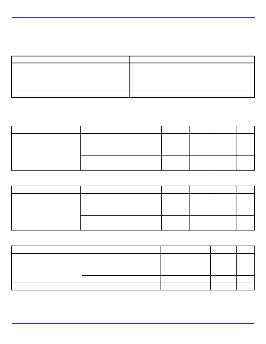
Absolute Maximum Ratings
NOTE: Stresses beyond those listed under Absolute Maximum Ratings may cause permanent damage to the device. These ratings are stress
specifications only. Functional operation of product at these conditions or any conditions beyond those listed in the DC Characteristics or AC
Characteristics is not implied. Exposure to absolute maximum rating conditions for extended periods may affect product reliability.
DC Electrical Characteristics
Table 4A. Power Supply DC Characteristics, VDD = VDDO = 3.3V ± 5%, TA = -40°C to 85°C
Table 4B. Power Supply DC Characteristics, VDD = VDDO = 2.5V ± 5%, TA = -40°C to 85°C
Table 4C. Power Supply DC Characteristics, VDD = 3.3V ± 5%, VDDO = 2.5V ± 5%, TA = -40°C to 85°C
Item
Rating
Supply Voltage, VDD
4.6V
Inputs, VI
-0.5V to VDD + 0.5V
Outputs, VO
-0.5V to VDD + 0.5V
Package Thermal Impedance,
θ
JA
74.9
°C/W (0 mps)
Storage Temperature, TSTG
-65
°C to 150°C
Symbol
Parameter
Test Conditions
Minimum
Typical
Maximum
Units
VDD
Power Supply Voltage
3.135
3.3
3.465
V
VDDO
Output Supply Voltage
3.135
3.3
3.465
V
IDD
Power Supply Current
PWR_DN = 1
77
mA
PWR_DN = 0
<1
mA
IDDO
Output Supply Current
12
mA
Symbol
Parameter
Test Conditions
Minimum
Typical
Maximum
Units
VDD
Power Supply Voltage
2.375
2.5
2.625
V
VDDO
Output Supply Voltage
2.375
2.5
2.625
V
IDD
Power Supply Current
PWR_DN = 1
68
mA
PWR_DN = 0
<1
mA
IDDO
Output Supply Current
10
mA
Symbol
Parameter
Test Conditions
Minimum
Typical
Maximum
Units
VDD
Power Supply Voltage
3.135
3.3
3.465
V
VDDO
Output Supply Voltage
2.375
2.5
2.625
V
IDD
Power Supply Current
PWR_DN = 1
77
mA
PWR_DN = 0
<1
mA
IDDO
Output Supply Current
10
mA
发布紧急采购,3分钟左右您将得到回复。
相关PDF资料
ICS84021AYLF
IC SYNTHESIZER HIGH FREQ 32-LQFP
ICS840245AGILF
IC FREQ SYNTHESIZER 16-TSSOP
ICS8402AYILF
IC FREQ SYNTHESIZER 32-LQFP
ICS841602AGILF
IC CLOCK GENERATOR 28-TSSOP
ICS841608AKI
IC CLOCK GENERATOR 32-VFQFPN
ICS841S012DKILF
IC FREQ SYNTHESIZER 56VFQFN
ICS842023BGLF
IC CLK GEN ETHERNET 25MHZ 8TSSOP
ICS8421002AGILF
IC FREQ SYNTHESIZER 20-TSSOP
相关代理商/技术参数
ICS840022AKI-02LFT
功能描述:IC CLOCK GENERATOR 16VFQFPN RoHS:是 类别:集成电路 (IC) >> 时钟/计时 - 时钟发生器,PLL,频率合成器 系列:HiPerClockS™, FemtoClock™ 标准包装:1,000 系列:- 类型:时钟/频率合成器,扇出分配 PLL:- 输入:- 输出:- 电路数:- 比率 - 输入:输出:- 差分 - 输入:输出:- 频率 - 最大:- 除法器/乘法器:- 电源电压:- 工作温度:- 安装类型:表面贴装 封装/外壳:56-VFQFN 裸露焊盘 供应商设备封装:56-VFQFP-EP(8x8) 包装:带卷 (TR) 其它名称:844S012AKI-01LFT
ICS840024AGI
制造商:ICS 制造商全称:ICS 功能描述:FEMTOCLOCKS⑩ CRYSTAL-TO LVCMOS/LVTTL FREQUENCY SYNTHESIZER
ICS840024AGILF
功能描述:IC FREQ SYNTHESIZER 20-TSSOP RoHS:是 类别:集成电路 (IC) >> 时钟/计时 - 时钟发生器,PLL,频率合成器 系列:HiPerClockS™, FemtoClock™ 标准包装:1,000 系列:- 类型:时钟/频率合成器,扇出分配 PLL:- 输入:- 输出:- 电路数:- 比率 - 输入:输出:- 差分 - 输入:输出:- 频率 - 最大:- 除法器/乘法器:- 电源电压:- 工作温度:- 安装类型:表面贴装 封装/外壳:56-VFQFN 裸露焊盘 供应商设备封装:56-VFQFP-EP(8x8) 包装:带卷 (TR) 其它名称:844S012AKI-01LFT
ICS840024AGILFT
功能描述:IC FREQ SYNTHESIZER 20-TSSOP RoHS:是 类别:集成电路 (IC) >> 时钟/计时 - 时钟发生器,PLL,频率合成器 系列:HiPerClockS™, FemtoClock™ 标准包装:1,000 系列:- 类型:时钟/频率合成器,扇出分配 PLL:- 输入:- 输出:- 电路数:- 比率 - 输入:输出:- 差分 - 输入:输出:- 频率 - 最大:- 除法器/乘法器:- 电源电压:- 工作温度:- 安装类型:表面贴装 封装/外壳:56-VFQFN 裸露焊盘 供应商设备封装:56-VFQFP-EP(8x8) 包装:带卷 (TR) 其它名称:844S012AKI-01LFT
ICS840024AGIT
制造商:ICS 制造商全称:ICS 功能描述:FEMTOCLOCKS? CRYSTAL-TO LVCMOS/LVTTL FREQUENCY SYNTHESIZER
ICS840024I
制造商:ICS 制造商全称:ICS 功能描述:FEMTOCLOCKS⑩ CRYSTAL-TO LVCMOS/LVTTL FREQUENCY SYNTHESIZER
ICS840031AMI
制造商:ICS 制造商全称:ICS 功能描述:FEMTOCLOCKS? CRYSTAL-TO LVCMOS/LVTTL FREQUENCY SYNTHESIZER
ICS840031AMILF
功能描述:IC CLOCK GENERATOR 8-SOIC RoHS:是 类别:集成电路 (IC) >> 时钟/计时 - 时钟发生器,PLL,频率合成器 系列:HiPerClockS™, FemtoClock™ 标准包装:1,000 系列:- 类型:时钟/频率合成器,扇出分配 PLL:- 输入:- 输出:- 电路数:- 比率 - 输入:输出:- 差分 - 输入:输出:- 频率 - 最大:- 除法器/乘法器:- 电源电压:- 工作温度:- 安装类型:表面贴装 封装/外壳:56-VFQFN 裸露焊盘 供应商设备封装:56-VFQFP-EP(8x8) 包装:带卷 (TR) 其它名称:844S012AKI-01LFT